


Description
TB67H420FTG Dual/Single Motor Driver Carrier
The TB67H420FTG Dual/Single Motor Driver Carrier breaks out the H-bridge motor driver IC onto a simple to use board. Capable of bidirectional control of up to two DC motors between 10-47V. Able to supply a continuous current of 1.7A to two seperate motors or around 3.4A to a single motor, it can also cope with peak currents of 4.5A per channel or 9A to a single motor for a few seconds. This is an excellent choice when running small or medium sized motors which run at high voltages!
Dual/Single Motor Driver Carrier Features
- Single- or dual-channel H-bridge motor driver (can drive one or two DC motors)
- Motor supply voltage: 10 V to 47 V
- Output current:
- up to 1.7 A continuous (4.5 A peak) per motor in dual-channel mode
- up to 3.4 A continuous (9 A peak) in single-channel mode
- Configurable current chopping actively limits motor current to 4.5 A per channel (dual) or 9 A (single) by default; can be lowered with external resistors or voltage sources
- No separate logic supply needed; inputs are 3V- and 5V-compatible
- Flexible input interface provides several options for control
- Under-voltage lockout and protection against over-current/short-circuit and over-temperature
- Open-load detection
- Carrier board adds reverse-voltage protection up to 40 V
- Active-low error outputs indicate over-current, over-temperature, or open-load condition
- Compact size (1.0″ × 1.2″)
- Exposed solderable ground pad below the driver IC on the bottom of the PCB
Included Kit
- TB67H420FTG Dual/Single Motor Driver Carrier Board
- 1×20-pin breakaway 0.1″ male header
- 3 x 2-pin, 3.5 mm terminal blocks
Truth Tables
| TB67H]420FTG simplified truth table | |||||
|---|---|---|---|---|---|
| Inputs | Outputs | Operation | |||
| INx1 | INx2 | PWMx | x+ | x− | |
| 1 | 0 | PWM | PWM (H/L) | L | forward/brake at speed PWM % |
| 0 | 1 | L | PWM (H/L) | reverse/brake at speed PWM % | |
| 1 | 0 | 0 | L | L | brake low (outputs shorted to ground) |
| 0 | 1 | ||||
| 1 | 1 | X | |||
| 0 | 0 | X | Z | Z | coast (outputs floating/disconnected) (standby if all IN and PWM inputs are low) |
| TB67H420FTG complete truth table | |||||
|---|---|---|---|---|---|
| Inputs | Outputs | Operation | |||
| PWMx | INx1 | INx2 | x+ | x− | |
| 0 | 0 | 0 | Z | Z | coast (standby if all IN and PWM inputs are low) |
| 1 | 0 | L | L | brake low | |
| 0 | 1 | ||||
| 1 | 1 | ||||
| 1 | 0 | 0 | Z | Z | coast |
| 1 | 0 | H | L | forward | |
| 0 | 1 | L | H | reverse | |
| 1 | 1 | L | L | brake low | |
Pinout
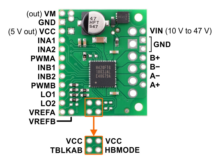
| PIN | Default State | Description – dual channel mode (HBMODE = LOW) |
Description – single channel mode (HBMODE = HIGH) |
|---|---|---|---|
| VIN | 10 V to 47 V board power supply input (reverse-protected up to 40 V). | ||
| GND | Ground connection points for the motor and logic supplies. The control source and the motor driver must share a common ground. | ||
| VM | These pins give access to the motor power supply after the reverse-voltage protection MOSFET (see the board schematic below). They can be used to supply reverse-protected power to other components in the system. VM is generally intended as an output, but it can also be used to supply board power, and some of the VM and GND holes are spaced for the addition of an optional through-hole capacitor. | ||
| A+ | Motor A output +. | Motor output A (connect together). | |
| A− | Motor A output −. | ||
| B+ | Motor B output +. | Motor output B (connect together). | |
| B− | Motor B output −. | ||
| VCC | Regulated 5 V output: this pin gives access to the voltage from the internal regulator of the TB67H420FTG. The regulator can only provide a few milliamps, so the VCC output should only be used for logic inputs on the board, not for powering external devices. | ||
| INA1 | LOW | Control input for A+. PWM can be applied to this pin (typically done with PWMA high). | Control input for A+ and A−. PWM can be applied to this pin (typically done with PWMA high). |
| INA2 | LOW | Control input for A−. PWM can be applied to this pin (typically done with PWMA high). | Control input for B+ and B−. PWM can be applied to this pin (typically done with PWMA high). |
| PWMA | LOW | PWM input for channel A. | PWM input. |
| INB1 | LOW | Control input for B+. PWM can be applied to this pin (typically done with PWMB high). | Not used. |
| INB2 | LOW | Control input for B−. PWM can be applied to this pin (typically done with PWMB high). | Not used. |
| PWMB | LOW | PWM input for channel B. | Not used. |
| LO1 | HIGH | Error output 1: drives low when an over-current or over-temperature fault occurs. Otherwise, the board pulls this pin up to VCC. | |
| LO2 | HIGH | Error output 2: drives low when an open-load or over-temperature fault occurs. Otherwise, the board pulls this pin up to VCC. | |
| VREFA | Current chopping threshold reference for channel A. | Current chopping threshold reference. | |
| VREFB | Current chopping threshold reference for channel B. | Not used. | |
| TBLKAB | LOW | Blanking time configuration input (see datasheet). This input should not be changed while the board is powered. | |
| HBMODE | LOW | H-bridge drive mode configuration input: LOW selects dual-channel mode; HIGH selects single-channel mode. This input should not be changed while the board is powered. | |
Dual/Single Motor Driver Carrier Documents
- Toshiba TB67H420FTG datasheet (460k pdf)
- Schematic diagram of the TB67H420FTG Dual/Single Motor Driver Carrier (158k pdf)
- Dimension diagram of theTB67H420FTG Dual/Single Motor Driver Carrier (184k pdf)
- 3D model of the TB67H420FTG Dual/Single Motor Driver Carrier (4MB step)
- Drill guide for the TB67H420FTG Dual/Single Motor Driver Carrier (57k dxf)
Related Products


TB9051FTG Single Brushed DC Motor Driver Carrier
Pololu
£11.50
TB9051FTG Single Brushed DC Motor Driver Carrier
The TB9051FTG Single Brushed DC Motor Driver Carrier is a single-channel H-Bridge Motor breakout board that has the capability for bidirectional...


Stepper Motor Driver Carrier STSPIN820
Pololu
£17.00
Stepper Motor Driver Carrier STSPIN820 - Pololu 2878
This product is a carrier board or breakout board for the STSPIN820 stepper motor driver from STMicroelectronics (ST); we therefore recommend...


A4988 Stepper Motor Driver Carrier
Pololu
£15.50
A4988 Stepper Motor Driver Carrier - Pololu 1182
The A4988 stepper motor driver carrier is a breakout board for Allegro’s easy-to-use A4988 microstepping bipolar stepper motor driver and is a...


TB67S2x9FTG Stepper Motor Driver Carriers
£10.00 - £22.00
TB67S2x9FTG Stepper Motor Driver Carriers
This product is a carrier board or breakout board for Toshiba’s TB67S2x9FTG family of stepper motor drivers; we therefore recommend careful reading of the...

")
A4988 Stepper Motor Driver Carrier, Black Edition
Pololu
£18.00
A4988 Stepper Motor Driver Carrier, Black Edition
This is a carrier board for Allegro's A4988 DMOS Driver with translator and overcurrent protection. This stepper motor driver allows you to control...